It took the semiconductor industry over a decade to prep everything needed for production of chips using extreme ultraviolet (EUV) lithography. It looks like it is going to take a lot less to reach the next level — EUV with High-NA.
Higher Resolution Needed
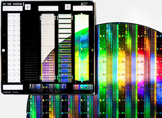
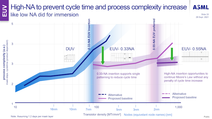
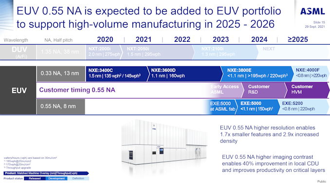
Nowadays the most advanced chips are made on 5/4-nm-class process using EUV lithography ASML's Twinscan NXE:3400C (and similar) systems that feature a 0.33 numerical aperture (NA) optics, which provides a 13 nm resolution. This resolution is good enough for a single-pattern approach at 7 nm/6 nm nodes with 36 nm ~ 38 nm pitches and at 5nm with 30 nm ~ 32 nm pitches. But as pitches get below 30 nm (at beyond 5 nm nodes) the 13 nm resolution might call for dual lithographic exposure that is going to be used for years to come.
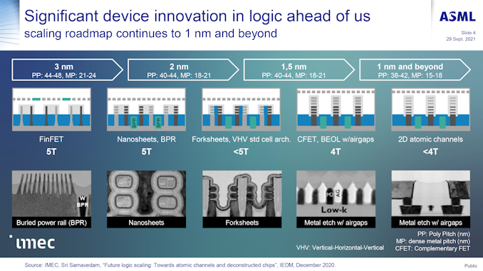
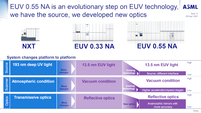
For post-3nm nodes, ASML and its partners are working on a brand-new EUV tool — the Twinscan EXE:5000-series — featuring a 0.55 NA (High-NA) lens capable of an 8nm resolution, which is projected to avoid multipatterning at 3 nm and beyond. The new High-NA scanners are still in development, they are expected to be extremely complex, very large, and expensive — each of them will cost over $400 million. High-NA will require not only new optics, but a new light source too, and even new fab buildings to accomodate the larger machines, which will require major investments.
But in a bid to keep scaling performance, power, area, and costs (PPAc) of semiconductors, leading makers of logic chips and memory devices are willing to adopt new technologies, and High-NA EUV scanners are crucially important for post 3-nm nodes. As a result, demand for High-NA tools is, well, pretty high.
10 to 20 High-NA Systems to Be Delivered
Several weeks ago, ASML disclosed that it had received multiple orders in Q1 2022 for its High-NA Twinscan EXE:5200 systems (EUV 0.55 NA) from both logic and DRAM customers. Last week it clarified that it had five orders for pilot High-NA scanners due to be delivered in 2024 and 'over five' orders for subsequent models featuring higher productivity that will be delivered starting from 2025, reports Reuters.
Interestingly, back in 2020 ~ 2021, ASML said that it had has received High-NA commitments from three customers, for a total of up to 12 systems. Keeping in mind that logic makers are usually the first to adopt leading edge tools, it is safe to bet that Intel, Samsung Foundry, and TSMC committed in 2020 ~ 2021 to get pre-production High-NA scanners. Moreover, ASML has already started building the first High-NA system, which will be completed in 2023 and will be used by Imec and ASML customers for research and development purposes.
"On High-NA EUV, we are making good progress and have currently started the integration of the first High-NA system in our new cleanroom in Veldhoven," said Peter Wennink, chief executive of ASML. "We received multiple orders for our EXE:5200 system in Q1. We also received additional EXE:5200 orders this month, April. With these bookings, we now have High-NA orders from three Logic and two Memory customers. The EXE:5200 is ASML's next model High-NA system and will provide the next step for lithography performance and productivity."
ASML's Twinscan EXE:5200 is considerably more complex than regular Twinscan NXE:3400C machines, so it takes longer time to build these tools. The company hopes that it will be able to deliver as many as 20 High-NA systems in mid-term future, which probably means that its customers will have to compete for these machines.
"We are also discussing with our supply chain partners to secure a capacity of around 20 EUV 0.55NA systems in the medium term," said Wennink.
Intel First to Adopt Pre-Production Tools
So far, the only process technology confirmed to use ASML's High-NA tools is Intel's 18A node and that one was once scheduled to enter high-volume production in 2025, around the time when ASML starts to deliver its production High-NA EUV systems. But recently Intel pulled-in the start of18A production to the second half of 2024 and indicated that it could use ASML's Twinscan NXE:3600D or NXE:3800E for its 18A manufacturing, presumably via multi-patterning.
While Intel's 18A technology would greatly benefit from High-NA EUV tools, it looks like Intel does not necessarily need Twinscan EXE:5200 machines for this node. Usage of multi-patterning for commercial chips means a longer product cycle, lower productivity, higher risks, and potentially lower yields (though the latter is not cast in stone). Yet, it looks like Intel wants its 18A node to arrive as soon as possible, perhaps because it considers it a major tool that will allow it to recapture process technology leadership from TSMC. Consequently, Intel's updated plans are now to phase in High-NA tooling during 18A's lifecycle if the tools are completed on time.
Of course, it remains to be seen whether usage of 0.33 NA EUV scanners for 18A will offer enough productivity for Intel and customers of Intel Foundry Services. But, at least in 2024, Intel is not going to have any choice but to use machines that it has.
Other leading makers of semiconductors — TSMC, Samsung, SK Hynix, and Micron — will also inevitably adopt High-NA EUV for high-volume manufacturing of chips. The only question is when exactly this is when exactly this is set to happen.