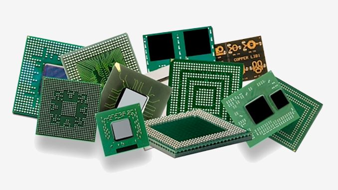
As the chip industry develops more sophisticated processors with higher heat dissipation requirements, some firms have moved on to chiplet-based designs. This not-so-gradual shift has resulted in chip packaging technologies becoming increasingly important. Large and highly complex chips such as Nvidia's H100 and advanced multi-chip solutions like Intel's Data Center Max GPU (Ponte Vecchio) present new requirements for packaging materials. To that end, Dai Nippon Printing (DNP) is showcasing a new development for semiconductor packages – Glass Core Substrate (GCS) – which it says can address many of those challenges.
Typically, modern chips are installed on fine pitch substrates (FPS), which are then put on multi-layer high-density interconnect (HDI) substrates. The most advanced CPU/GPU HDI substrates these days use Ajinomoto Build-up Film(ABF), which combines organic epoxy resins, hardener, and inorganic microparticle filler, according to the manufacturer. It is easy to use, and it can achieve high-density pitching (thus enabling high density metal wiring), it has insulation properties that are good enough for modern chips, high rigidity, high durability, and low thermal expansion, among other factors.
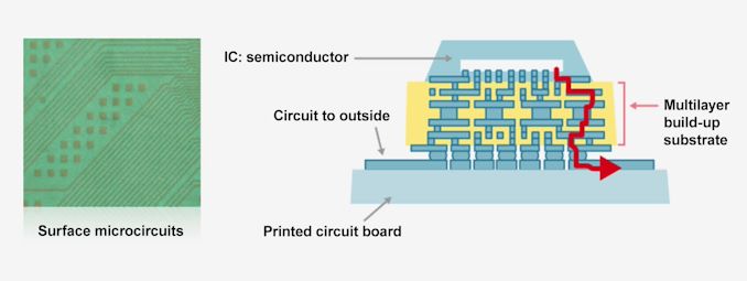
Will ABF and other organic resin-based substrates still be good enough for chiplets? Well, it's quite a challenge, as these multi-chiplet designs will be more power-hungry (and thus hotter) and require metal writing of a higher density due to the widening of memory and I/O interfaces. This increase in power requirements puts added pressure on the outlying substructure of the circuitry. Finding new materials to use within the core makeup of chips within the semiconductor industry has been a hot pursuit for many years.
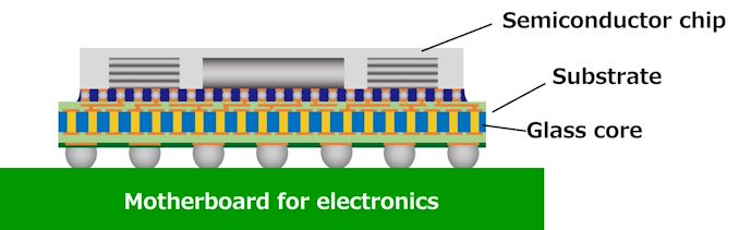
One such company in the semiconductor industry is Dai Nippon Printing (DNP), and they claim that their HDI substrates with a glass core have superior properties compared to organic resin-based substrates. According to Dai Nippon, using a glass core substrate (GCS) can enable finer pitching and, therefore, extremely dense wiring because it is stiffer and less prone to expansion due to high temperatures. A schematic drawing demonstrated by DNP even omits the fine pitch substrate from the packaging altogether, implying that this part may no longer be needed.
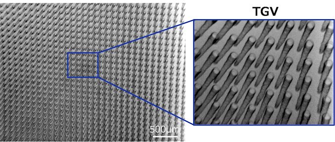
Perhaps, most notably, DNP claims its glass core substrate can offer high through glass via (TGV) density (compatible with FPS) with a high aspect ratio. The aspect ratio, in this case, is the ratio between the thickness of the glass and the diameter of the via. As the number of vias increases and the ratio increases, the processing of substrates gets harder, and maintaining the rigidity gets more challenging.
Glass is considered more rigid than organic resin-based substrates and has several advantages, but the adhesion between glass and copper (or other metal wires) is still a major challenge in regard to bonding. The DNP-developed glass substrate has an aspect ratio of 9 and ensures adhesiveness to enable fine pitch-compatible wiring. Since there are only a few GCS thickness constraints, there is a lot of freedom when it comes to maintaining a balance between thickness, warpage, stiffness, and smoothness, the company says.
Dai Nippon Printing produces out-coupling enhancement structures for LCDs and scattering for backlighting modules, so it has vast experience with the mass production of glass-based structures. Meanwhile, DNP is not the only specialist in rigid glass applications looking ahead to the future in making HDI substrates for advanced chips or multi-chiplet solutions. Corning has been exploring this area for quite a while, though it does not look like its technology is used commercially for high-volume chips or in multi-chip-modules.
Source: Dai Nippon Printing